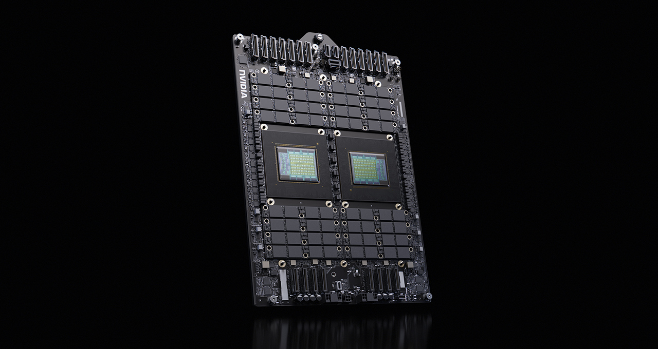
NVIDIAがVera CPUを活用して次世代CPUおよびGPUの設計を加速NVIDIA Harnesses Vera CPU to Speed Up Design of Next-Generation CPUs and GPUs
匿名の公開いいねです。記事の保存・お気に入りではなく、Featured、Top 3、重要度、掲載順位には影響しません。仕組みとプライバシーAnonymous public likes are reactions, not saved articles or bookmarks. They do not affect Featured, Top 3, importance, or listing order.How it works and privacy
- NVIDIAは自社開発のVera CPUをEDAワークフローに投入し、次世代チップ設計の演算処理を大幅に高速化した。
- 自社シリコンで設計プロセス自体を効率化する取り組みとして注目される。
NVIDIA is deploying its Vera CPU to accelerate EDA workloads used in designing next-generation chips, demonstrating that its own silicon can dramatically speed up the chip development process itself.
本ページの本文と要約は AI による自動生成です。日本語版と英語版は言語ごとに独立して生成されるため、表現や詳しさが異なる場合があります。正確性は元記事 (blogs.nvidia.com) をご確認ください。The body and summaries are AI-generated independently for each language, so wording and detail may differ. Verify accuracy at the original source (blogs.nvidia.com).
要約と収集メタデータに基づく AI 解説。元記事全文の転載・翻訳ではありません。AI explainer based on the summaries and collected metadata, not a copy or translation of the full source article.
NVIDIAは、自社開発のVera CPUを次世代CPUおよびGPUの設計に使うEDAワークフローへ投入し、演算処理を大幅に高速化した。複雑さを増す現代のチップ設計に対し、高性能なCPUアーキテクチャで開発作業を加速する取り組みとなる。
Vera CPU
CPU、GPU、AIシステムが高度化するにつれ、それらを開発するエンジニアリングチームが扱う設計も複雑になっている。NVIDIAはこの課題に対応するため、Vera CPUを活用。次世代CPUとGPUの開発に用いる設計工程へ実際に配備し、要求の厳しいエンジニアリング処理を高速化できることを示している。
EDAワークフロー
Vera CPUの導入先は、半導体設計を支える電子設計自動化、すなわちEDAのワークフローだ。NVIDIAはCadenceおよびSynopsysと協力し、重要なEDAアプリケーションをVera CPU向けに最適化している。自社のシリコンを使ってチップそのものだけでなく、その設計プロセスの効率も高める構成であり、チップ生産のペースに関わる取り組みと説明されている。
検証と実装
半導体開発では、シミュレーション、検証、実装の各技術が中心的な役割を担う。Vera CPUによって、これらを含むEDA処理の負荷を高速に扱うことが狙いとなる。EDAワークロードの強化はチップ開発の進行を支え、それによって恩恵を受ける技術の開発テンポにもつながるとされる。
Modern Chip Design
NVIDIA is using its Vera CPU in the electronic design automation workflows that support development of its next generation of CPUs and GPUs. The effort matters because the growing complexity of modern chip design places increasing demands on the engineering workloads involved in producing more sophisticated CPUs, GPUs and AI systems.
The company says Vera can dramatically accelerate the computational work behind the chip development process itself. Its deployment also demonstrates how a high-performance CPU architecture can help speed up some of the industry’s most demanding engineering workloads.
Vera Across EDA Workflows
NVIDIA is collaborating with Cadence and Synopsys to optimize critical EDA applications for the Vera CPU. It is also deploying Vera across the EDA workflows used to design its own next-generation processors.
This approach applies NVIDIA’s own silicon to the process of developing future silicon. Rather than limiting Vera to a single part of that process, NVIDIA is introducing the CPU across workflows that contribute to CPU and GPU development. According to the announcement, the resulting acceleration can make the overall chip design process more efficient.
Simulation, Verification and Implementation
Simulation, verification and implementation technologies play central roles in semiconductor development. These are among the EDA workloads that must keep pace as chip designs become increasingly complex.
The broader issue is the pace of chip production. By boosting EDA workloads, Vera can help engineering teams move demanding design work forward more quickly. NVIDIA presents its use of Vera as a demonstration that faster CPU processing can accelerate the workflows behind next-generation chip development.
The announcement also connects stronger EDA performance with the tempo of technologies that depend on semiconductor development. Faster design workloads can support development momentum by improving the speed of the engineering processes used to create increasingly sophisticated chips and AI systems.
ポコとTECHガイドPoko & TECH Guide
ポコと当サイトのTECHガイドが、記事の要約と収集した情報から読みどころを語るAI生成の対話です。Poko and TECH Dashboard's own TECH Guide discuss the article's highlights in an AI-generated conversation based on its summary and collected source details.
- ポコPokoVera CPUをEDA作業に投入って、自分のCPUで次のCPUやGPUを設計するの? EDAって何?They’re using the Vera CPU to design their next CPUs and GPUs? What exactly is EDA?
- TECHガイドTECH GuideEDAはチップの設計や検証を助ける仕組みじゃ。この記事では、CadenceやSynopsysと重要アプリをVera向けに最適化し、設計工程へ展開しておる。EDA covers tools that help design and verify chips. The article says NVIDIA is working with Cadence and Synopsys to optimize key applications for Vera and deploy them across its design workflows.
- ポコPoko設計者にとって、道具を速くして図面作りから検査までテンポアップする感じ? 誰に役立つの?So for chip designers, it’s like speeding up the tools used from drafting through inspection? Who benefits from that?
- TECHガイドTECH Guide設計チームが行うシミュレーション、検証、実装の負担を軽くし、チップ開発のペースを上げる狙いじゃ。書かれている範囲では、関連技術の開発にも弾みがつくのう。It aims to ease demanding simulation, verification, and implementation work for design teams, accelerating chip development. As described, that faster pace could also build momentum for related technologies.
- ポコPokoつまり、自社CPUが次世代チップ開発の裏方まで加速するってことか。へえ、面白い!So NVIDIA’s own CPU is speeding up the behind-the-scenes work of building its next chips. That’s pretty neat!
- TECHガイドTECH Guideそうじゃ。押さえたいのは、半導体開発の中心となるシミュレーション、検証、実装にVeraを使い、高性能CPU設計が加速に役立つと本文が示している点じゃよ。Exactly. The article’s key point is that Vera is being applied to core semiconductor tasks—simulation, verification, and implementation—showing how a high-performance CPU architecture can help accelerate development.