XPUはいかにして世界クラスのAIファクトリーと融合するかHow XPUs Meet a World-Class AI Factory
匿名の公開いいねです。記事の保存・お気に入りではなく、Featured、Top 3、重要度、掲載順位には影響しません。仕組みとプライバシーAnonymous public likes are reactions, not saved articles or bookmarks. They do not affect Featured, Top 3, importance, or listing order.How it works and privacy
NVIDIAはNVLink Fusionを通じてXPUをAIファクトリーインフラに統合し、トークン毎秒・ワット効率・稼働率を最大化する一貫したファクトリー設計の重要性を示した。
NVIDIA outlines how XPUs can integrate into a cohesive AI factory via NVLink Fusion, emphasizing that maximizing tokens per second, efficiency, and uptime requires treating AI infrastructure as a unified system rather than discrete components.
本ページの本文と要約は AI による自動生成です。日本語版と英語版は言語ごとに独立して生成されるため、表現や詳しさが異なる場合があります。正確性は元記事 (blogs.nvidia.com) をご確認ください。The body and summaries are AI-generated independently for each language, so wording and detail may differ. Verify accuracy at the original source (blogs.nvidia.com).
要約と収集メタデータに基づく AI 解説。元記事全文の転載・翻訳ではありません。AI explainer based on the summaries and collected metadata, not a copy or translation of the full source article.
NVIDIAは公式ブログで、多様なプロセッサ「XPU」をNVLink Fusionを通じてAIファクトリーのインフラへ統合する手法を示した。AI基盤を個々の部品の寄せ集めではなく、一つの「工場」として設計・構築することが、大規模なAI運用の成否を分けるという主張だ。
同社が掲げる「AIファクトリー」という概念は、AIによる知能の生成をデータセンター規模の生産活動になぞらえたものだ。工場が休みなく稼働するように、AIファクトリーも継続的に動き続け、その経済性は「送り出される成果」で測られる。具体的には、1秒あたりの処理トークン数、消費電力あたりのトークン数(トークン毎ワット)、トークンあたりのコスト、そして設備の稼働率と可用性である。
こうした指標を最大化するには、演算装置単体の性能だけでなく、それらを結ぶネットワークやメモリ、電力設計まで含めた全体最適が欠かせない。NVIDIAは、GPUやCPU、専用アクセラレータといった多様な演算装置を総称する「XPU」を高速インターコネクトのNVLink Fusionでつなぐことで、システム全体を一体として動かす狙いを示している。個別のコンポーネントを寄せ集めるのではなく、統合されたシステムとして扱うことが、効率と稼働率の向上に直結するという考え方だ。
背景には、生成AIの普及に伴う推論需要の増大がある。学習だけでなく、実際にモデルを動かして応答を返す推論の段階でも膨大な計算資源が求められ、電力効率やコスト効率が事業採算を左右するようになってきた。同種の取り組みは業界全体で進んでおり、独自のAIアクセラレータを開発するクラウド事業者も増えていると見られる。多様なチップを柔軟に組み込める接続技術は、こうした流れの中で重要性を増していく可能性がある。
NVLink Fusionは、NVIDIA以外の演算装置も自社のインターコネクト網に組み込めるようにする枠組みと位置づけられる。今回のブログは、単体のチップ性能競争から、データセンター全体をどう設計するかという「システム設計」の競争へと軸足が移りつつある状況を映し出していると言えそうだ。
NVIDIA has published a technical overview describing how custom accelerators, which it refers to broadly as XPUs, can be integrated into large-scale AI data centers through its NVLink Fusion interconnect technology. The topic matters because the economics of modern AI infrastructure increasingly depend not on the raw specifications of any single chip but on how efficiently an entire facility converts power and silicon into usable model output.
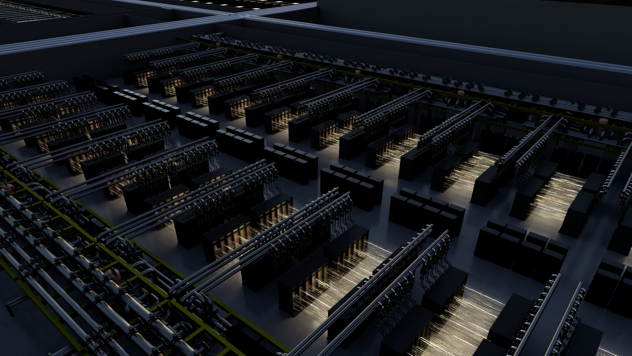
At the center of NVIDIA's framing is the concept of an "AI factory," a term the company uses to describe data centers purpose-built to generate intelligence at scale rather than to run conventional enterprise workloads. According to the company, these facilities operate continuously, and their economics are defined by delivered output measured in metrics such as tokens per second, tokens per watt, cost per token, utilization and uptime. In this view, effective AI infrastructure must be designed and built as a full factory, not a collection of independently optimized parts. The argument is that isolated component improvements do not necessarily translate into better system-level performance if the surrounding architecture, interconnect and software are not aligned.
NVLink is NVIDIA's high-bandwidth, low-latency interconnect, originally developed to link GPUs together so that many processors can behave more like a single, larger computing resource. This matters for large AI models, where the work of training or serving is spread across many accelerators that must exchange data constantly. Bottlenecks in that communication can leave expensive silicon idle, reducing utilization and raising the effective cost per token. NVLink Fusion extends this ecosystem beyond NVIDIA's own GPUs, allowing partners to connect their own custom silicon, whether XPUs or CPUs, into NVIDIA's rack-scale systems and the broader NVLink fabric.
The strategic implication is notable. Many large cloud providers and chip designers have been developing bespoke accelerators tailored to their specific workloads, seeking greater efficiency or reduced dependence on a single supplier. By offering NVLink Fusion, NVIDIA appears to be positioning its interconnect and system architecture as the connective tissue for these heterogeneous designs, rather than requiring every component to be a NVIDIA GPU. In practice this means a customer's custom XPU could sit alongside NVIDIA hardware within the same coherent, rack-scale system, drawing on shared networking, memory access patterns and software tooling.
This fits into a wider industry pattern in which the unit of design has shifted from the chip to the rack and, increasingly, to the entire data center. NVIDIA has previously described rack-scale platforms built around its Grace CPUs and Blackwell GPUs, connected by NVLink switching, as examples of this integrated approach. Supporting technologies in the same ecosystem include high-speed networking such as InfiniBand and Ethernet-based fabrics, along with software layers for orchestration, scheduling and monitoring that aim to keep accelerators busy and power draw predictable. The emphasis on tokens per watt also reflects the growing importance of energy efficiency and power availability, which have become practical constraints on how quickly new AI capacity can be deployed.
For organizations building or renting AI capacity, the framing carries a clear message: raw compute is only one input, and the returns on a facility are shaped by how well all elements work together over sustained periods of operation. Metrics like uptime and utilization underline that reliability and consistent throughput are commercial concerns, not just engineering ones, because idle or underused hardware directly erodes the value of a costly installation.
It is worth noting that this is a vendor overview from NVIDIA's own blog, so the perspective is naturally aligned with the company's product strategy. The extent to which custom XPUs from third parties will be adopted through NVLink Fusion, and how they will perform against alternative interconnect and integration approaches, is likely to depend on real-world deployments, pricing and the willingness of large operators to standardize on NVIDIA's fabric. Even so, the underlying trend the piece describes, treating AI infrastructure as a unified system engineered for delivered output rather than a set of discrete components, reflects a broadly recognized direction in how large-scale AI data centers are now being planned and evaluated.
ポコとTECHガイドPoko & TECH Guide
ポコと当サイトのTECHガイドが、記事の要約と収集した情報から読みどころを語るAI生成の対話です。Poko and TECH Dashboard's own TECH Guide discuss the article's highlights in an AI-generated conversation based on its summary and collected source details.
- ポコPokoXPUとAIファクトリーが「融合」するって、つまりどういうこと? NVLink Fusionもよく分からないな。What does it mean for XPUs to “merge” with an AI factory? And what exactly is NVLink Fusion?
- TECHガイドTECH Guide簡単に言うとじゃな、XPUは処理装置を幅広く指す言葉じゃ。記事によれば、NVLink FusionでそれらをAI基盤へ統合する構想じゃよ。Put simply, XPU is a broad term for processing units. According to the article, NVLink Fusion integrates them into the broader AI infrastructure.
- ポコPoko部品をまとめてつなぐと、何がうれしいの? 個別に高性能なら十分じゃないのかな。What’s the benefit of connecting everything together? Wouldn’t individually powerful components be enough?
- TECHガイドTECH Guide記事の要点は、AI基盤を部品の寄せ集めでなく一つの工場として設計することじゃ。秒間トークン数や電力効率、稼働率の最大化を目指せるわけじゃな。The article’s point is to design AI infrastructure as one factory, not a pile of parts. That approach aims to maximize tokens per second, power efficiency, utilization, and uptime.
- ポコPokoなるほど! XPU単体だけでなく、AIファクトリー全体を一つの仕組みとして考えるのが大事なんだね。Got it! The key isn’t just the XPU itself—it’s treating the entire AI factory as one coordinated system.
- TECHガイドTECH Guideその通りじゃ。今後の見どころは、NVLink Fusionによる統合設計が、記事の挙げた出力・効率・稼働の指標にどう結びつくかじゃな。Exactly. The key thing to watch is how NVLink Fusion’s unified design connects to the article’s measures of output, efficiency, utilization, and uptime.