AIコンピュートのスケーリングに新しい電力アーキテクチャが必要な理由Why Scaling AI Compute Performance Requires a New Power Architecture
匿名の公開いいねです。記事の保存・お気に入りではなく、Featured、Top 3、重要度、掲載順位には影響しません。仕組みとプライバシーAnonymous public likes are reactions, not saved articles or bookmarks. They do not affect Featured, Top 3, importance, or listing order.How it works and privacy
- AIファクトリーの高密度化に伴い、従来の電力配電方式では非効率が生じているため、NVIDIAは800VDCアーキテクチャへの移行を推進している。
- これによりラック単位での電力損失を削減し、大規模GPUクラスタの性能向上を支える。
NVIDIA outlines why traditional AC power distribution struggles to keep pace with modern AI compute density, and makes the case for an 800V DC power architecture that reduces conversion losses and enables more efficient scaling of GPU-dense AI factories.
本ページの本文と要約は AI による自動生成です。日本語版と英語版は言語ごとに独立して生成されるため、表現や詳しさが異なる場合があります。正確性は元記事 (blogs.nvidia.com) をご確認ください。The body and summaries are AI-generated independently for each language, so wording and detail may differ. Verify accuracy at the original source (blogs.nvidia.com).
要約と収集メタデータに基づく AI 解説。元記事全文の転載・翻訳ではありません。AI explainer based on the summaries and collected metadata, not a copy or translation of the full source article.
AIコンピュート
新世代のアクセラレーテッドコンピューティングでは、計算性能だけでなく、ラック密度や電力供給の効率、拡張性も重要になる。NVIDIAは、AIファクトリーの高密度化に従来のAC電力配電方式が追いつきにくくなっていると説明している。
電力面のボトルネックは、単純なワット数だけではない。電力がグリッドからGPUへ届くまでの経路と、その途中で生じる非効率が課題とされる。
800VDC
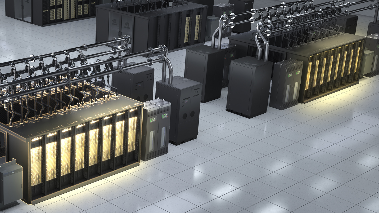
NVIDIAが移行を推進しているのが、800VDC電力アーキテクチャだ。電力変換に伴う損失を減らし、ラック単位の配電をより効率化することで、高密度なGPUを備えるAIファクトリーの拡張を可能にすると説明されている。
この構成は、大規模GPUクラスタを支える電力供給の効率と拡張性を高め、性能向上を下支えするものと位置付けられている。
AI Compute Density
NVIDIA says scaling AI compute requires a new approach to power architecture because traditional AC power distribution struggles to keep pace with modern compute density. As accelerated computing advances, the underlying infrastructure must provide more compute performance, support higher rack density and distribute power more efficiently at scale.
Grid to the GPU
According to the source, the constraint is not simply the total wattage available. The key issue is how power moves from the grid to the GPU. As AI factories become denser, conventional power distribution can introduce inefficiencies, including conversion losses at the rack level.
800V DC Power Architecture
NVIDIA is making the case for a transition to an 800V DC power architecture. The described approach is intended to reduce power-conversion losses and enable more efficient scaling in GPU-dense AI factories. By improving rack-level power distribution, the architecture is positioned as infrastructure that can support the performance requirements of large-scale GPU clusters.
ポコとTECHガイドPoko & TECH Guide
ポコと当サイトのTECHガイドが、記事の要約と収集した情報から読みどころを語るAI生成の対話です。Poko and TECH Dashboard's own TECH Guide discuss the article's highlights in an AI-generated conversation based on its summary and collected source details.
- ポコPokoAIを使う仕事やサービスって、普段の何が変わるの?電気の仕組みが変わるだけで、性能にも効くの?What changes in everyday work or services that use AI? Can changing the power setup really affect performance?
- TECHガイドTECH Guideこの記事では、800VDCでラックの電力損失を減らし、大規模GPUクラスタの性能向上を支えるとしておる。まずAI工場の土台が効率化する話じゃ。The article says 800V DC can cut rack-level power losses and support large GPU clusters. The immediate change is a more efficient foundation for AI factories.
- ポコPokoへえ、前の電力配電ではできなかったの?ACとDCって何が違うの?Wow, couldn’t the old power distribution setup do that? And what’s the difference between AC and DC?
- TECHガイドTECH Guideできなかったというより、高密度化に追いつきにくかったのじゃ。本文では従来のAC配電は変換損失が課題で、ACは交流、DCは直流じゃよ。Not impossible, but harder to keep up with rising density. As the piece explains, traditional AC distribution faces conversion losses; AC is alternating current, while DC is direct current.
- ポコPokoなるほど。一番の収穫は、GPUを増やすだけじゃなく、電気の届け方も性能を左右するってことだね!Got it. My biggest takeaway is that performance depends not only on adding GPUs, but also on how power reaches them!
- TECHガイドTECH Guideそうじゃ。記事が注目しているのは、800VDCへの移行で損失をどこまで抑え、高密度なAI工場を効率よく拡大できるかじゃのう。Exactly. The piece focuses on whether moving to 800V DC can curb losses and help dense AI factories scale more efficiently.